An introduction to the chip industry and where it’s headed with 2.5D and 3D-IC.
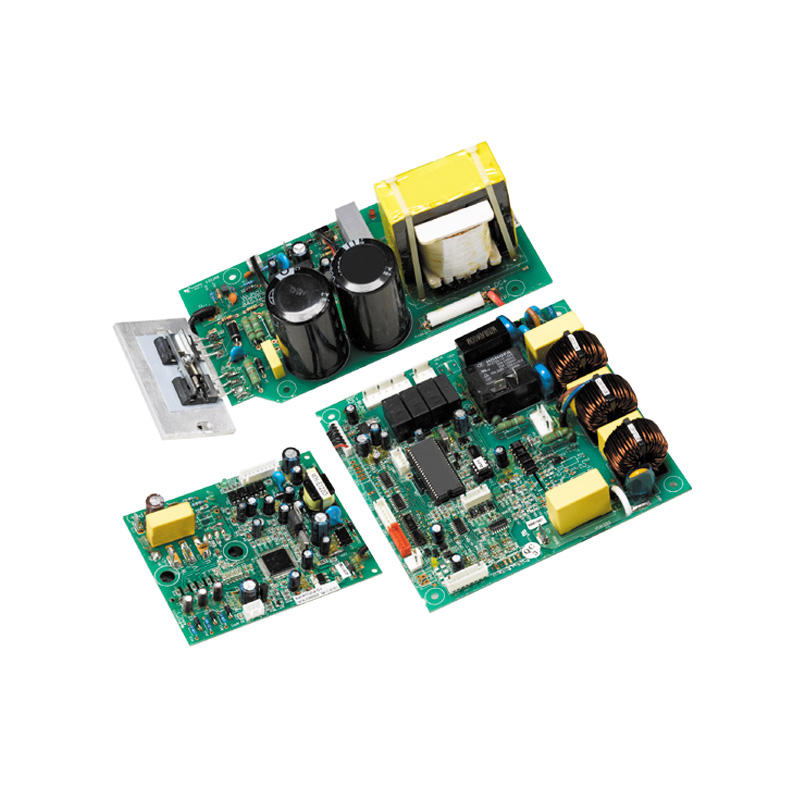
In our modern world, just about everything is woven together by electronics. From microwaves to satellites, electronics-powered devices are infused into our every waking moment. Today, even our sleep includes digital acoustics, haptics, and analytics. But while the systems that light, connect, and move our lives can vary greatly, nearly every electronic device has one or more of the same fundamental building block — the very small and very complex integrated circuit. Jlcpcb Flex Pcb
An integrated circuit (IC) — commonly called a chip — is made out of a semiconductor material called silicon, in which small electronic components called transistors are formed within the silicon and then wired together with interconnects layered on top of the silicon surface.
You’re probably familiar with the little black boxes nestled neatly inside your favorite devices. With their diminutive size and unassuming characteristics, it can be hard to believe these vessels are actually the linchpin of most modern electronics. But without integrated chips, most technologies would not be possible, and we — as a technology-dependent society — would be helpless.
Integrated circuits are compact electronic chips made up of interconnected components that include resistors, transistors, and capacitors. Built on a single piece of semiconductor material, such as silicon, integrated circuits can contain collections of hundreds to billions of components — all working together to make our world go ‘round.
The uses of integrated circuits are vast: children’s toys, cars, computers, mobile phones, spaceships, subway trains, airplanes, video games, toothbrushes, and more. Basically, if it has a power switch, it likely owes its electronic life to an integrated circuit. An integrated circuit can function within each device as a microprocessor, amplifier, or memory.
Integrated circuits are created using photolithography, a process that uses ultraviolet light to print the components onto a single substrate all at once — similar to the way you can make many prints of a photograph from a single negative. The efficiency of printing all the IC’s components together means ICs can be produced more cheaply and reliably than using discrete components. Other benefits of ICs include:
ICs have been making increasingly sophisticated devices possible for nearly 75 years. But how did they begin? The idea of putting several components on one chip was first considered in the 1950s, with different scientists being credited with independently developing similar designs at approximately the same time.
Since their creation, integrated circuits have gone through several evolutions to make our devices ever smaller, faster, and cheaper. While the first generation of ICs consisted of only a few components on a single chip, each generation since has prompted exponential leaps in power and economy.
The first IC manufacturers were vertically integrated companies that did all the design and manufacturing steps themselves. This is still the case for some companies like Intel, Samsung, and memory chip manufacturers. But since the 1980s, the “fabless” business model has become the norm in the semiconductor industry.
A fabless IC company does not manufacture the chips they design. Instead, they contract this out to dedicated manufacturing companies that operate fabrication facilities (fabs) shared by many design companies. Industry leaders like Apple, AMD, and NVIDIA are examples of fabless IC design houses. Leading IC manufacturers today include TSMC, Samsung, and GlobalFoundries.
ICs can be classified into different types based on their complexity and purpose. Some common types of ICs include:
After designing and manufacturing a chip, there is a third and final step in which the chip is tested and packaged. This is one more highly specialized subfield in the semiconductor industry.
Because the actual silicon chip is too small and delicate to manipulate directly, IC packaging provides something more substantial to work with. A protective casing — typically an enclosure made of plastics or ceramics with integrated leads or bumps — enables us to connect the tiny chip to a circuit board. Depending on the intended application, IC packaging can vary in size and shape.
Some common IC packages include:
As consumption of everything digital continues to put pressure on devices to be faster, smarter, and smaller, the need for ICs to process more information more efficiently is never-ending. In the most recent generation, there are two very promising new options: the 2.5D and 3D-IC.
In 2.5D-ICs, two or more chips are placed next to each other, on the same surface plane, in a technique called interposer technology. This side-by-side proximity across a shared base increases the interconnect density.
Now take that logic a level up, literally, and you have 3D-ICs. This logic-on-logic sandwich is created by stacking chips or wafers on top of each other. In addition to increasing the interconnection even more, 3D-ICs offer more processing power in a smaller footprint and are highly flexible for using different technology nodes.
A major new challenge posed by these multi-die packaging technologies is heat dissipation. When you consider that a high-performance computing (HPC) chip can easily consume over 200 watts, it becomes obvious that overheating and thermal management are major limiting factors when you start stacking several of these chips closely together.
By making ICs more efficient in how they connect, 2.5D and 3D technologies are overcoming the scaling challenge that engineers have been tackling since the 1950s: “How do we get more with less?”
By enabling engineers to predict the performance of ICs, accurate signoff verification is critical to optimizing the design process for nearly every electronic device. With simulation, designers can evaluate their ICs against several requirements, including power consumption, thermal, and parametric yield. In addition, Ansys RedHawk-SC is uniquely equipped to provide comprehensive multiphysics analysis, revealing how different physics will interact to affect the IC’s performance and longevity.
To learn more about integrated circuits, register for our webinar “Thermal Integrity Challenges and Solutions of Silicon Interposer Design.“
Name* (Note: This name will be displayed publicly)
Alu Pcb Email* (This will not be displayed publicly)